New Funding Fuels Acceleration of Optical I/O Roadmap Supporting Generative AI, Machine Learning and HPC Applications
Ayar Labs, a leader in silicon photonics for chip-to-chip connectivity, today announced it has raised an additional $25 million in Series C1 funding, bringing its total Series C raise to $155 million. The oversubscribed up round was led by new investor Capital TEN. VentureTech Alliance also entered the Series C expansion that included participation by previous investors Boardman Bay Capital Management, IAG Capital Partners, NVIDIA, and Tyche Partners. Existing strategic and financial investors include Applied Ventures, GlobalFoundries, Hewlett Packard Pathfinder, Intel Capital and Lockheed Martin Ventures.
This press release features multimedia. View the full release here: https://www.businesswire.com/news/home/20230524005128/en/

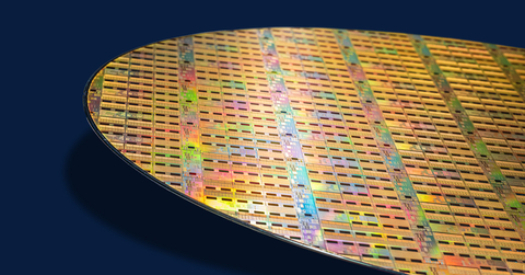
Photo of Ayar Labs TeraPHY™ optical I/O chiplet wafer. Photo courtesy of Ayar Labs.
“We believe that future computing solutions will include large-scale use of silicon photonics for data communications, and have been following Ayar Labs for some time now,” said Pin-Nan Tseng, General Partner at Capital TEN. “Given our deep expertise in the semiconductor industry and the Taiwan semiconductor ecosystem, we believe Ayar Labs has the technology solution, people, capital, and broad support to lead in the transition from copper to optical interconnects for scale-out computing and memory applications.”
Ayar Labs’ patented optical I/O approach uses industry-standard, cost-effective silicon processing techniques to replace traditional electrical I/O with fast, high-density, low power optical I/O chiplets and multi-wavelength light sources. Moving data between chips using light instead of electricity breaks the performance, power, and distance limitations of copper interconnect, critical for latency-sensitive applications such as high performance computing, AI and machine learning. Optical I/O will also impact other areas that require rapid transfer of data, such as cloud and data center, telecommunications, and aerospace and defense.
“We’re extremely pleased with the ongoing interest and financing we’ve received from leaders in the semiconductor industry,” said Charles Wuischpard, CEO of Ayar Labs. “This C1 adds sophisticated investor partners that will allow us to accelerate our strategic roadmap, and is further validation of our technology and plan to bring silicon photonics-based interconnect solutions to market at scale.”
Ayar Labs will use the funds to accelerate the implementation and commercialization of its optical I/O solutions to address the power consumption, latency, reach and system bandwidth bottlenecks that threaten future advances in generative AI, while also expanding the company's product offerings and development efforts.
NVIDIA, which participated in Ayar Labs’ earlier Series C raise in April 2022, increased its investment in the company.
“NVIDIA is reimagining the data center with integrated hardware, software and networking for accelerated computing,” said Craig Thompson, Vice President of Business Development, Networking Business Unit at NVIDIA. “Generative AI models with trillions of parameters are accelerating demand for this platform, which is why we are increasing our investment in Ayar Labs.”
Recently named one of America’s Best Startup Employers by Forbes, the funds will also help the company increase hiring plans by up to 50 percent this year. Ayar Labs has received a number of other accolades in recent months. The company was recognized as an honoree in Fast Company’s most recent “Next Big Things in Tech” awards. In addition, Mark Wade, Ayar Labs’ Co-Founder, CTO and Senior Vice President of Engineering, was recently appointed to Global Semiconductor Alliance’s CTO Council. Wade was also recently named to Electro Optics’ inaugural “The Photonics 100 2023” list.
About Ayar Labs
Ayar Labs is using light to disrupt traditional compute power and performance curves, enabling the next design breakthroughs for the growth of generative AI, disaggregated data centers, 6G, phased array sensory systems and more. Ayar Labs’ patented approach uses silicon photonics techniques to replace traditional electrical-based I/O with high-speed, highly efficient optical interconnect chiplets and multi-wavelength light sources. The company was founded in 2015 and is funded by a number of domestic and international venture capital firms, as well as strategic investors such as GlobalFoundries, Hewlett Packard Pathfinder, Intel Capital, Lockheed Martin Ventures and NVIDIA. For more information, visit www.ayarlabs.com.
View source version on businesswire.com: https://www.businesswire.com/news/home/20230524005128/en/
Contacts
Kristine Raabe, press@ayarlabs.com


